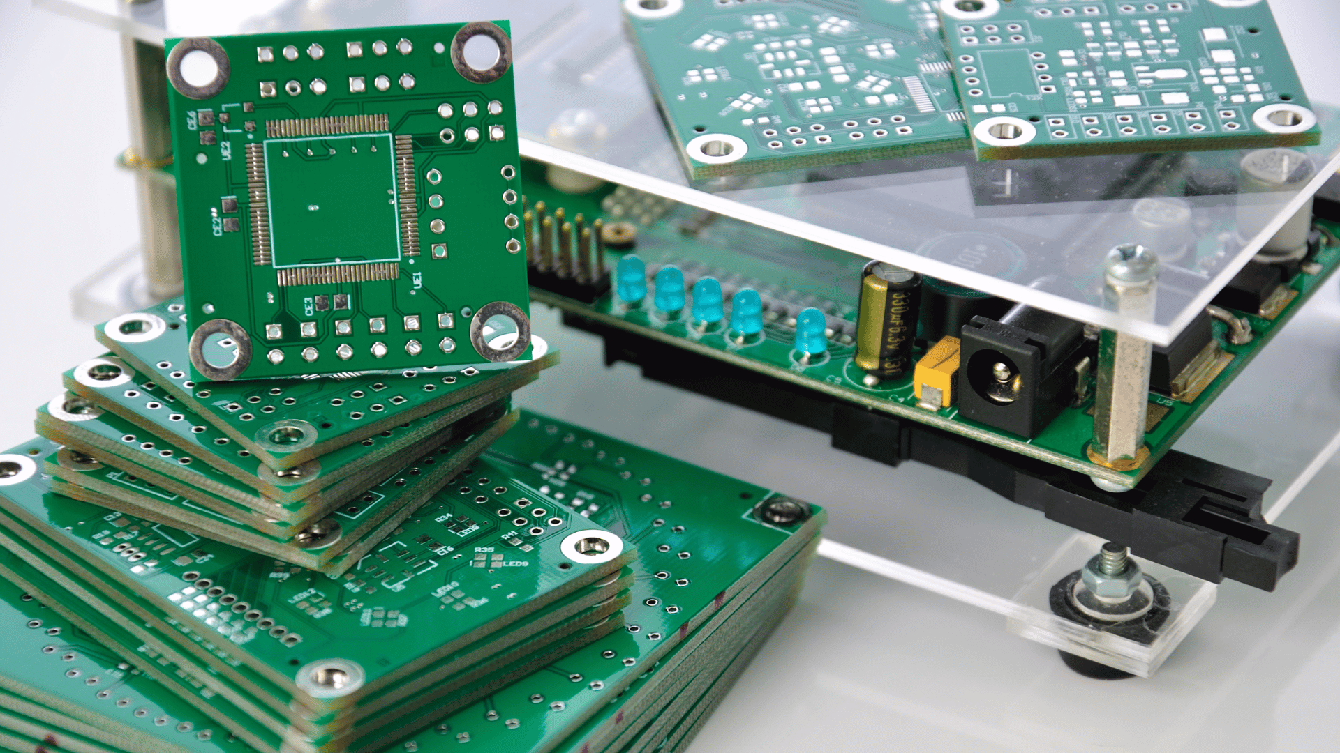
Printed circuit boards (PCBs) are used in nearly all electronic devices so it’s crucial to assess their quality before integrating them into electronic systems. There are many methods for checking PCB quality, but the most popular method involves using X-ray scanners. With X-ray scanners, manufacturers can identify hidden defects and other quality-related issues without causing any damage to the PCBs.
Issues with PCB Inspection
Inspection of modern PCBs can be challenging due to several reasons. Firstly, the boards and their components are much smaller, making it increasingly difficult to inspect thoroughly. Additionally, there is a greater number of components on each board. To accommodate this increasing density, modern PCBs have complex layouts with more layers. Solder joints and components may be hidden between the inner layers of the PCB or within the final product.
The shrinking size and intricate layout make manual inspections impossible as quality control teams are not able to see tiny details or peer between layers. Automated optical inspection (AOI) is a common PCB inspection method, but it is not effective for boards with a lot of components because the components can be hidden or shadowed. X-ray scanners are more effective because they can penetrate the layers of PCBs, enabling manufacturers to inspect solder joints and identify defects.
How Do X-Ray Scanners Work?
X-ray scanners are popular for inspecting PCBs because they allow manufacturers see every inch of the PCB, including between layers and underneath components. Here’s a brief and very simple overview on how X-ray scanners work:
- X-Ray Generation: The scanners are equipped with a high-voltage generator that emits X-ray beams that can penetrate through various materials.
- X-Ray Detection: When X-rays pass through an object, the object absorbs some of their energy. Different materials with varying densities will absorb different levels of energy. Detectors on the opposite side of the machine measure the remaining energy of the X-rays.
- Imaging: The computer converts the data collected by the detector into an image that shows the composition of the scanned items. Generally, dense and heavier elements like metals absorb more energy, appearing darker on an X-ray image. Less dense items like plastic appear lighter.
- Visualization: The image is displayed on the monitor so quality inspection personnel can identify defects or inconsistencies.
What Can X-Ray Scanners Find?
Metallic components appear darker in X-ray images whereas other materials like glass, plastic, and silicon look lighter. With an X-ray scanner, inspectors can see all the components on a PCB and identify issues such as:
- Solder Bridges: This occurs when an excessive amount of solder is applied, leading to a connection of solder joints or a “bridge” where there should not be one.
- Solder Voids: A solder void is an empty space or hole within the solder joint, caused by entrapped air, flux residue, or cured resin in the solder paste. These voids reduce the thermal conductivity of solder joints.
- BGA Open Circuit: This is a defect that occurs when there is a break or gap in one or more of the electrical connections between the ball grid array (BGA) component and the PCB. This can lead to a loss of electrical connectivity.
- Delamination: Delamination refers to the separation or detachment of layers within the board.
Benefits of X-Ray Inspection
With X-ray scanners, manufacturers are able to find more defects in less time, resulting in increased efficiency and reliable electronic devices.
Identifies Defects
X-ray scanners can reveal hidden defects that may not be visible to the naked eye. By detecting these faults, manufacturers can determine the cause and make necessary corrections to prevent future reoccurrences. X-ray inspection also enables them to ensure that their PCBs meet strict quality standards, reducing the risk of product malfunctions. As a result, end-users receive electronic devices that are dependable and built to last.
Nondestructive Testing
With X-ray scanners, quality control teams can thoroughly inspect PCBs without having to take apart the layers or employ alternative methods that might damage the boards. Doing this saves time and resources by eliminating the need for disassembling and reassembling the boards. It also ensures that the PCBs won’t undergo an additional process that could introduce more defects.
Accelerates Inspection Process
X-ray scanners automate the inspection process, enabling quality control teams to assess X-ray images without having to disassemble the boards or rely on manual inspections. This automation streamlines the inspection process, enabling manufacturers to examine more PCBs in a shorter timeframe. X-ray inspection also reduces the likelihood of human errors which enhances overall quality control.
PCB Inspection Solutions from 2M Technology
PCBs are the core of electronic devices and installing a defective PCB in a device can lead to malfunctions or even complete failure. If you are a PCB manufacturer, you can use X-ray scanners to check PCBs before they are dispatched for the production of electronic devices. Likewise, if you are involved in the production of electronic devices, X-ray scanners can serve as a pre-scanning solution for assessing PCBs before they are incorporated into your products. This proactive approach guarantees the quality of your products, whether they are PCBs themselves or electronic devices that rely on PCBs.
To get started on your PCB X-ray inspection solution, contact the 2M Technology sales team at +1 (214) 988-4302 or at sales@2mtechnology.net. You can also use the links below to chat with a sales consultant directly or request a free live demo or quote of one of our X-ray scanners.

