Electronics Manufacturing
X-Ray Inspection Systems
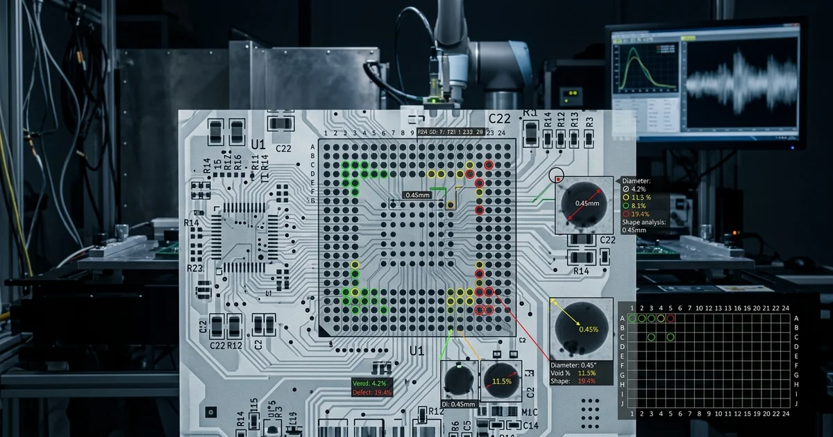
BGA solder void analysis, PCB solder joint inspection, wire bond verification, and component placement confirmation for electronics production lines. 2M Technology engineers X-ray inspection systems that identify defects invisible to automated optical inspection — at production speed, with AI-powered classification that reduces escapes and false calls simultaneously.
What is Electronics Manufacturing X-Ray Inspection?
Electronics manufacturing X-ray inspection is the application of 2D and 3D X-ray imaging systems to verify the internal quality of electronic assemblies — including PCB solder joints, ball grid array (BGA) interconnects, wire bonds, flip-chip connections, and package seals — at points in the manufacturing process where visual or optical inspection cannot access the inspection target. X-ray inspection is essential for BGA and QFN packages where solder joints are hidden beneath the component body, and for multi-layer PCB assemblies where internal layer connections cannot be verified by surface inspection alone. AI-powered X-ray inspection classifies solder defects with greater consistency than human operators and generates quantitative void percentage and joint geometry data for process engineering.
Maximum BGA solder void area percentage per IPC-A-610 Class 3 (military/aerospace) — X-ray is the only inspection method capable of measuring void percentage in hidden solder joints
Minimum feature size detectable with high-resolution 2D X-ray inspection on PCB assemblies — enabling detection of hairline cracks, micro-voids, and incomplete solder wetting invisible to optical systems
Computed tomography X-ray provides cross-sectional imaging of solder joints, enabling measurement of joint height, shape, and internal void structure — the gold standard for BGA process validation
The global acceptability standard for electronic assemblies — IPC-A-610 Class 2 (commercial) and Class 3 (high-reliability) define specific X-ray inspection criteria for BGA void, solder coverage, and joint geometry
X-Ray Inspection vs. Automated Optical Inspection (AOI)
Automated optical inspection (AOI) is the standard first-pass quality check on SMT lines. X-ray inspection is the essential second layer that catches defect types AOI physically cannot detect — not because AOI is inferior, but because it cannot see through components or into hidden solder joints.
| Defect Type | AOI | 2D X-Ray | 3D CT X-Ray |
|---|---|---|---|
| BGA solder void | No | Yes (2D area %) | Yes (3D volume %) |
| BGA missing ball | No | Yes | Yes |
| Cold solder joint (surface) | Partial | Yes | Yes |
| Solder bridge (hidden) | No | Yes | Yes |
| Component misplacement | Yes | Yes | Yes |
| QFN / LGA solder coverage | No | Yes | Yes |
| Wire bond integrity | No | Yes | Yes |
| Joint height measurement | No | No | Yes |
| Conformal coating coverage | Yes (UV) | No | No |
Electronics X-Ray Inspection Applications
BGA and QFN Inspection
Ball grid array and quad-flat no-lead packages have solder joints completely hidden under the package body after reflow. X-ray is the only non-destructive method to verify joint formation, detect voids, confirm ball count, and identify bridges in these packages. AI-powered BGA inspection automatically measures void percentage per ball, calculates total void area, and classifies assemblies against IPC-A-610 Class 2 or Class 3 criteria without operator measurement.
Through-Hole and PTH Solder Inspection
Plated through-hole (PTH) solder joint fill level verification requires X-ray imaging to confirm solder has wicked through the barrel and formed a concave fillet on the secondary side. AOI can inspect the primary side fillet but cannot confirm barrel fill. 2D X-ray imaging confirms barrel fill percentage and detects insufficient solder, blow holes, and cold joints in wave-soldered through-hole assemblies.
Wire Bond and Flip-Chip Inspection
Wire bond inspection verifies bond wire routing, loop height, and bond pad attachment in semiconductor packages and hybrid circuits. X-ray detects broken bonds, missing bonds, wire sweep, and excessive loop sag that indicate reliability risks in automotive, aerospace, and medical device electronics. Flip-chip underfill inspection confirms complete underfill coverage without voids that create thermal cycling failure points.
3D CT for Process Validation
3D computed tomography X-ray provides cross-sectional imaging at any plane through a PCB assembly, enabling measurement of solder joint height, shape, and internal void structure with micron-level resolution. 3D CT is used for new product introduction (NPI) process validation, failure analysis, and first-article inspection of complex assemblies where 2D X-ray cannot resolve overlapping features on multi-layer boards.
Inline vs. Offline Inspection
Inline X-ray systems integrate directly into the SMT production line, inspecting every board immediately after reflow at production speed. Offline systems inspect sampled boards or boards flagged by AOI, providing higher image resolution and 3D capability at lower throughput. 2M Technology sizes inspection architecture based on production volume, defect risk profile, and quality escape tolerance — not all applications require 100% inline inspection.
AI-Powered Defect Classification
AI defect classification models trained on electronics X-ray image libraries automatically categorize detected anomalies as BGA void, cold joint, bridge, missing component, or measurement within acceptable limits — eliminating operator-to-operator variation in pass/fail decisions. AI systems also generate quantitative void percentage measurements, joint geometry data, and SPC trend data that process engineers use to optimize reflow profiles and solder paste volume.
Electronics X-Ray System Specifications
| Parameter | 2D Inline System | 2D Offline System | 3D CT System |
|---|---|---|---|
| X-ray source energy | 80-130 kV | 80-160 kV | 130-225 kV |
| Resolution | 10-25 micron | 1-10 micron | 1-5 micron voxel |
| Throughput | 5-30 seconds/board | 2-10 minutes/board | 5-30 minutes/scan |
| Max board size | Up to 610 x 610 mm | Up to 610 x 610 mm | Component/module level |
| Primary use | 100% inline BGA inspection | Targeted/sample inspection | NPI, FA, validation |
| Output data | Pass/fail, void %, SPC | Image archive, measurements | 3D model, cross-sections, metrology |
Related Industrial Inspection Resources
Frequently Asked Questions: Electronics X-Ray Inspection
Engineer Your Electronics Inspection System
2M Technology designs and deploys 2D and 3D X-ray inspection systems for SMT, through-hole, wire bond, and advanced packaging electronics manufacturing. AI defect classification, IPC-A-610 compliance configuration, and SPC integration included.
(214) 988-4302 | sales@2mtechnology.net
